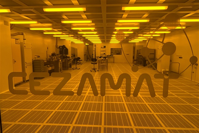
One of the largest high-tech R&D investment projects in Poland, the Centre for Advanced Materials and Technology (CEZAMAT) under the Warsaw University of Technology has been a pillar underpinning the semiconductor ambitions of Poland, especially the country's vibrant photonics ecosystem. Apart from the Warsaw University of Technology as consortium leader, CEZAMAT also includes Poland's Military University of Technologies, the University of Warsaw, and various institutes under the Polish Academy of Sciences.
Co-financed by the European Union and founded to enable the interdisciplinary development of research on modern materials and technologies, CEZAMAT operates a network of specialized laboratories. The Intelligent Semiconductor Systems Department under CEZAMAT, for example, has research teams dedicated to both planar semiconductor technologies as well as integrated photonics and houses various advanced equipment for academic and industry partners, including systems for wafer bonding, mask alignment, dry etching, electron beam lithography, and Chemical Vapour Deposition.
The integrated photonics team within CEZAMAT engages in basic and industrial R&D in the design, simulation, fabrication, and characterization of photonic integrated devices. Integrated photonic components operating in visible light, such as light guides, optical power dividers, and de-/multiplexers, have been fabricated on a silicon nitride (SiN) platform, alongside the development of indium phosphide (InP) and SOI-based photonic components. Notably, the use of electron beam lithography in the fabrication process allows the prototyping of photonic components and circuits without the need of photolithographic masks, thus enabling fast prototyping. Currently, on-site equipment allows the fabrication of 2, 4, and 8-inch substrates.
In May 2024, CEZAMAT jointly formed a Competence Centre for Microelectronics and Photonics together with Poland's Łukasiewicz Institute of Microelectronics and Photonics and Łukasiewicz Institute of Tele- and Radio Technology, with funding provided by Poland's National Recovery Plan. As part of the project, CEZAMAT will purchase new equipment in the existing laboratories, aiming to create a unique capability in Poland to manufacture photonic chips and microelectronic devices. Once completed, according to CEZAMAT, it will also be the only technology park in Central and Eastern Europe fully adapted to 8-inch substrates.
FAMES Consortium - one of the largest projects under the European Chips Act with EUR 830 million funding provided by participating member states and the Chips Joint Undertaking, also includes CEZAMAT as one of its four pilot lines that will develop new technologies such as FD-SOI at 10nm, 7nm and embedded non-volatile memories. The pilot lines will be accessible to all European universitities and companies. Spearheaded by the French semiconductor R&D institute CEA-Leti, the project also sees participation from other key players of European chip ecosystem, including Imec from Belgium, Fraunhofer Mikroelektronik from Germany, and Tyndall from Ireland.


